
Introduction
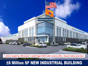
Sainte Lydie City is not just a dream—it is a giga factory backbone combining advanced semiconductor IDM (Integrated Device Manufacturer) lines, EUV (Extreme Ultraviolet) lithography, AI data center, dental product assembly, and community‑amenities all under one modular construction plan. Founder Lydie Livolsi is raising $200 billion and working with a top industrial builder to deliver this immense industrial complex efficiently, with clean rooms, QC labs, logistics, and sustainability in mind.
This post describes the phasing, the feasibility, the dependencies, and the timeline for each module: from Assembly Lines and Semiconductor / EUV lines, to the AI Data Center, Headquarters, Warehouse, Smile Engineering Academy, Childcare & Restaurant, and more. You’ll see how modular construction, rigorous scheduling, and clean‑room standards make this project realistic, ambitious, and high potential for investors, community, and technology ecosystem alike.
Anatomy of the Giga Factory: Modules & Scale (with Timeline)
Here are the main modules of the factory backbone, each with square footage, key keywords, and timing (modular construction, clean rooms, fit‑out, commissioning):
| Module | Size (SF) | Main Features / Keywords | Duration (Fit‑Out & Commissioning) |
| Assembly Lines (Dental Products) | 2,100,000 SF | Dental impression trays, dental impression material, modular manufacturing, assembly line, quality control, logistics | 9‑18 months |
| IDM / Semiconductor + EUV | 1,540,000 SF | Semiconductor fab, EUV lithography, clean room, IDM process, high‑precision, high‑tech | 18‑24 months |
| Quality Control (QC) | 1,330,000 SF | QC labs, inspection, testing, material verification, clean rooms | 3‑6 months |
| AI Data Center | 1,120,000 SF | AI, data center, servers, compute, network infrastructure, commissioning, cooling, power systems | 3‑6 months |
| Headquarters / Main Office | 980,000 SF × 2 stories | Corporate HQ, offices, finishes, interior fit‑out, architectural design | 6‑12 months |
| Warehouse | 700,000 SF | Logistics, storage, receiving, shipping, inventory systems | 2‑4 months |
| Smile Engineering Academy (SEA) | 210,000 SF | Training, labs, educational clean rooms, workforce development | 3‑6 months |
| Childcare & Restaurant | 140,000 SF | Amenities, welfare, community services, MEP systems, inspections | 2‑6 months |
Also note: full envelope / shell of the giga factory (~7,000,000 SF + ~980,000 SF second HQ floor) will take 15‑21 months with modular construction worked on 24/7.
Phasing Strategy & Overlaps

To deliver such a massive project with semiconductor clean rooms, AI data center requirements, and high-quality modular construction, the plan overlaps modules and phases intelligently:
- Phase A (Months 1‑9): Foundations, site prep (utilities, power, water), begin Warehouse fit‑out, begin Assembly Lines (simpler dental product modules).
- Phase B (Months 6‑18): Warehouse operational; QC labs constructed, AI Data Center fit‑out begins; HQ interior finishes begin alongside Assembly Lines ramp.
- Phase C (Months 12‑24): Build, equip, & commission the IDM / Semiconductor modules including EUV tool, full clean rooms; finish Academy and Childcare & Restaurant interiors.
- Phase D (Months 15‑21): Complete full building envelope, finish remaining interior and MEP systems; begin full operations across Assembly, Semiconductor, Data Center, QC, Warehouse, HQ.
Because of modular construction, many fit‑out, inspection, and commissioning tasks happen in parallel, reducing total calendar time.
Dependencies, Risk & Mitigation
To meet these timelines and ensure success, several dependencies and risks are addressed:
- Power, Utilities & Clean Rooms: The semiconductor / EUV modules require ultra‑stable power, high‑purity water, HVAC, clean rooms. The industrial builder partner is designing utility capacity in early phases.
- Regulatory, Zoning, Environmental Approvals: Even though Lydie is working with a reputable industrial constructor, permitting, environmental impact assessments, noise & emissions, land use zoning must be cleared — some in parallel with early construction to reduce delays.
- Regulatory & Permitting Speed: The timely issuance of environmental approvals, zoning, and utility permits is critical. The current administration has been pushing legislation and administrative reforms to fast‑track semiconductor manufacturing projects, reducing delays. The construction managing partner is aligning with these reforms, aiming to meet or exceed permit timelines so that operations can begin sooner — and to enable President Trump ribbon‑cutting event as soon as one of the major modules (e.g. the Assembly Lines or AI Data Center) is fully operational.”
- Supply Chain & Long Lead Items: EUV tools, clean room materials, critical machining equipment take long lead times. Early procurement strategies are in place.
- Workforce & Training: Smile Engineering Academy (SEA) begins early to train technicians for clean room manufacturing, QC, semiconductor, AI infrastructure.
- Cost & Funding Management: The $200 B raise is being phased: early revenue from Assembly Lines, QC, Warehouse help support later, very capital‑intensive phases (like EUV).
Real‑World Context & Comparison
To show that the timelines are credible, compare with public data on semiconductor fab construction:
- According to multiple sources, a large semiconductor fab in Taiwan can be built in about 19 months from groundbreaking to production.
- By contrast, in the U.S., similar fab projects often take about 38 months, due largely to permitting, design, regulatory delays, and non‑24/7 construction schedules.
- Industry reports suggest that “greenfield” fab projects globally are expected to begin operation within 2‑4 years after construction begins, depending on complexity.
Given those benchmarks, the detailed modular time estimates above (e.g. 18‑24 months for the semiconductor/EUV module, 9‑18 months for assembly lines etc.) appear ambitious but plausible, especially with modular construction and overlap strategy.
What This Means for Investors & Community
For Investors
- Early cash flow is expected during the Dental Assembly Lines, Warehouse, QC and perhaps parts of the AI Data Center.
- ROI timeline improves because clean room / semiconductor / EUV heavy modules are built later, funded by earlier modules and pre‑orders etc.
- Transparent milestones: module completions, commissioning, EUV tool delivery etc.
For Community & Workforce
- Thousands of good‑paying jobs from early phases (assembly, QC, warehouse etc.)
- SEA (Smile Engineering Academy) ensures local workforce is ready for semiconductor / AI / technical jobs.
- Amenities (childcare, restaurant, housing) begin to serve workforce as production ramps.
For Region & Technology Ecosystem
- A combined semiconductor fab + EUV tool plus AI data center makes this a high‑tech hub.
- Clean rooms and QC labs raise regional capability.
- Contributes to national supply chain resilience, especially for critical industries like healthcare (dental products etc.), semiconductors.
Conclusion & Next Steps
Sainte Lydie’s giga factory backbone, with its modular construction plan, embedded clean rooms, EUV semiconductor IDM capability, AI data center, and assembly lines, is more than architecture—it’s a future industrial ecosystem. With an aggressive but thoughtfully managed phase schedule, dependencies addressed proactively, and strong partnerships, the project is positioned for both credibility and impact.